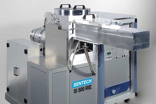
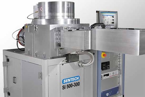
CP-RIE plasma etcher SI 500

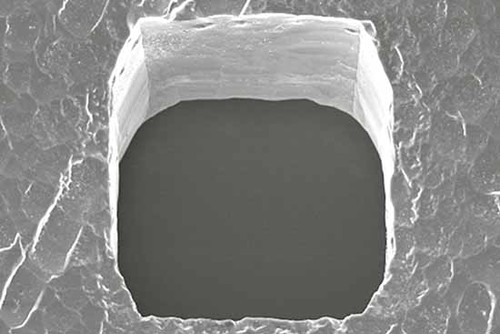
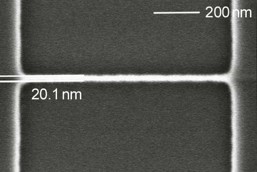
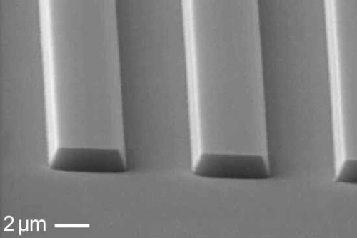
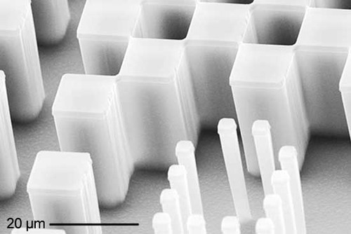
Low damage for nano structuring
Due to the low ion energy distribution, low damageetching and nano structuring can be performed with our icp plasma etching tools.
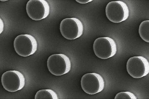
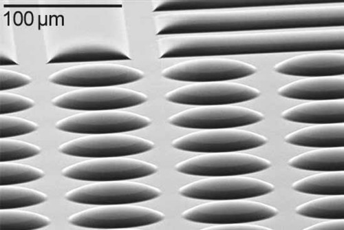
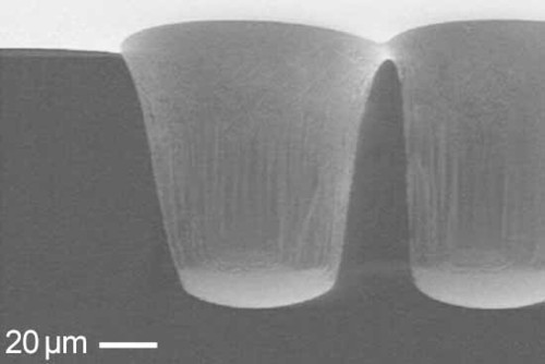
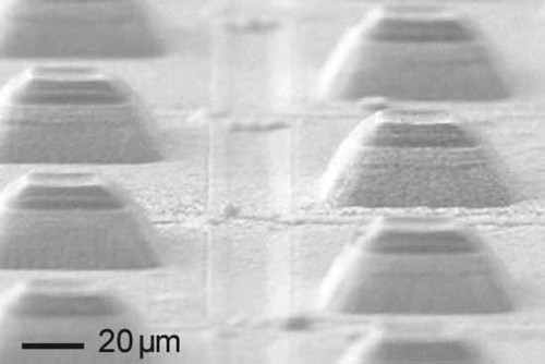
Simple high rate etching
High rate plasma etching of Si for MEMS with high aspect ratio is easily performed either using room temperature alternating processes or cryogenicprocesses for smooth side walls.
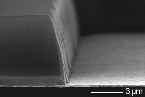
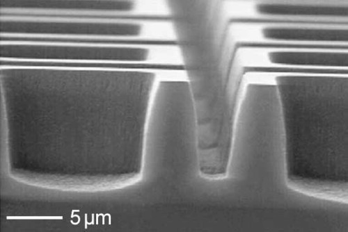
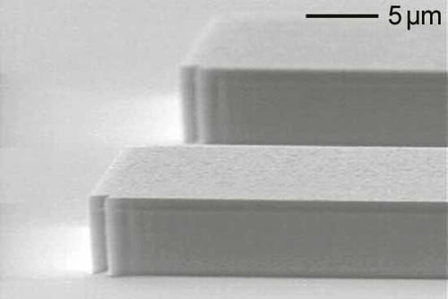
Inhouse ICP plasma source
The Planar Triple Spiral Antenna (PTSA) source is a unique feature of SENTECH high end plasma process systems. The PTSA source generates homogeneous plasma with high ion density and low ion energydistribution. It features high coupling efficiency and very good ignition behavior for processing of a large variety of materials and structures.
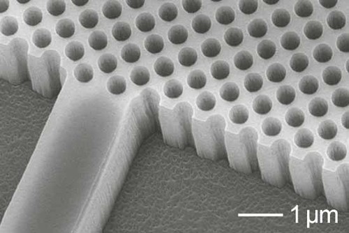
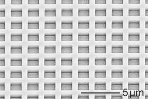
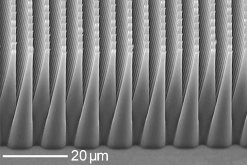
Dynamic temperature control
Substrate temperature setting and stability during the plasma etching processes are demanding criteria for high quality etching. The ICP substrate electrode with dynamic temperature control in combination with He backside cooling and substrate backside temperature sensing provides excellent process conditions over a wide temperature range from -150 °C up to +400 °C.
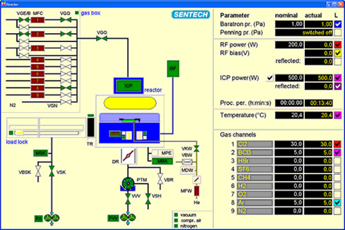
The SI 500 represents the leading edge for inductive coupled plasma (ICP) processing in research and production. It is based on the ICP plasma source PTSA, dynamic temperature controlled substrate electrode, fully controlled vacuum system, advanced SENTECH control software using remote field bus technology, and a very user-friendly general user interface for operating the SI 500. Flexibility and modularity are design characteristics of the SI 500.
A large variety of substrates from wafers up to 200 mm diameter to parts loaded on carriers can be processed in the SI 500 ICP plasma etching system. The single wafer vacuum loadlock guarantees stable process conditions and allows easy switch of processes.
The SI 500 ICP plasma etching tool can be configured for processing of a variety of materials, including but not limited to III-V compound semiconductors (GaAs, InP, GaN, InSb), dielectrics, quartz, glass, silicon, silicon compounds (SiC, SiGe), and metals.
SENTECH offers different levels of automation ranging from vacuum cassette loading to one process chamber up to six port cluster with different etch and deposition modules targeted to high flexibility or high throughput. The SI 500 ICP for plasma etching is available as process module on cluster configuration as well.