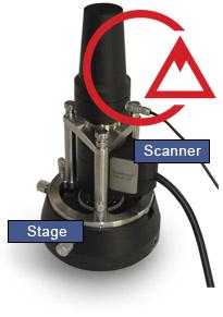
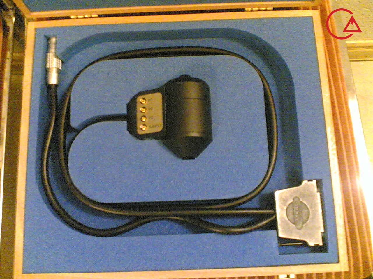
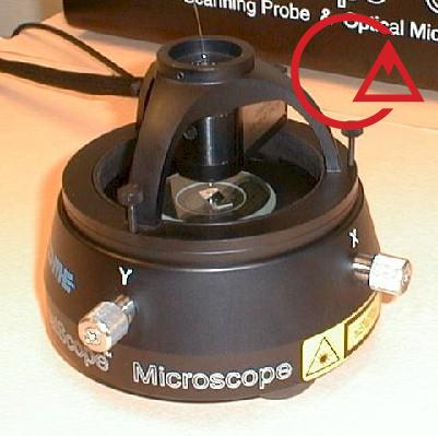
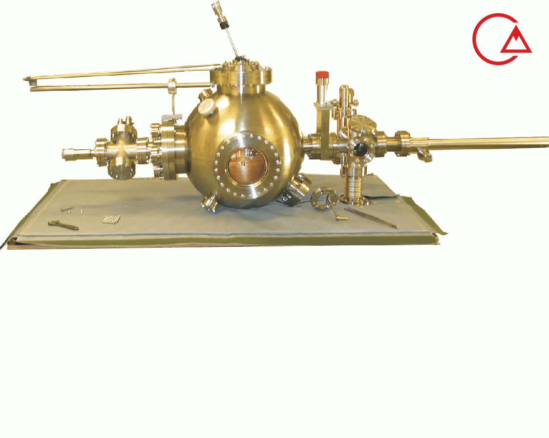
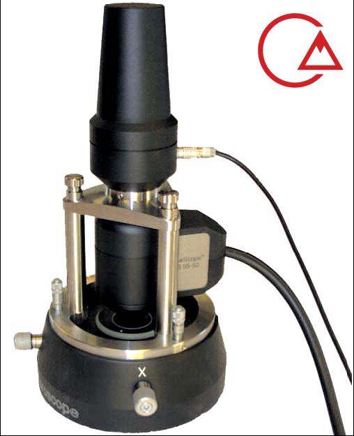
Combined tunnel scanning and atomic power (SPM) device
Getting to know the SPM device
Today, the importance of identifying and examining materials and systems using characterization systems in advanced technologies and research is considered as an important and unavoidable part.
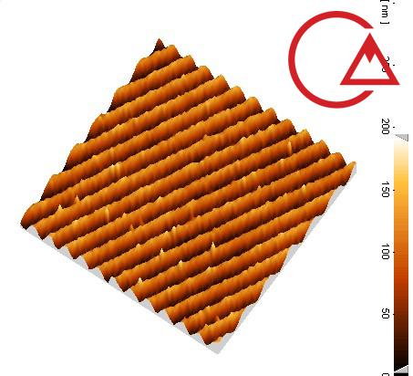
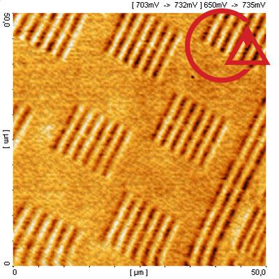
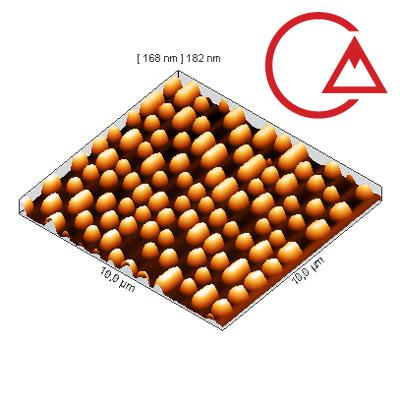
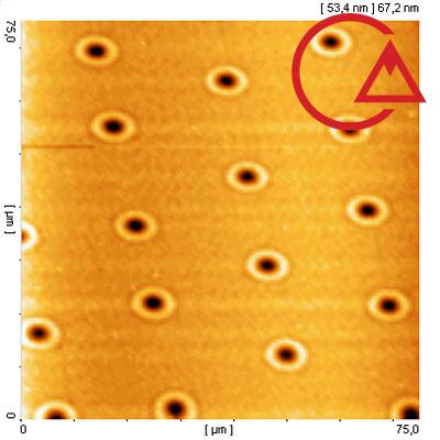
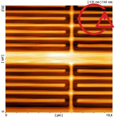
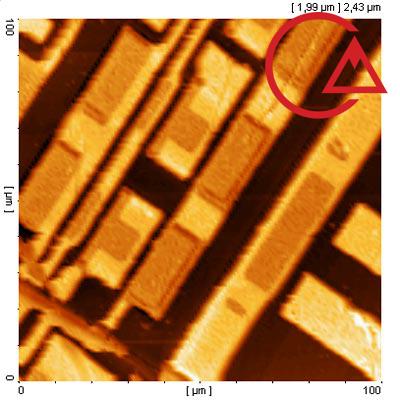
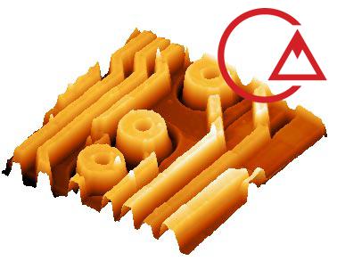
Scanning probe microscopes are one of the most practical characterization systems that, with a set of techniques, have the ability to examine the surface of materials with high resolution in the range of nanometers and even angstroms. In a general view, scanning probe microscopy (SPM) is a comprehensive title for a wide range of techniques that scan the surface of materials at the nano and even angstrom scale with a probe (needle) and topographic images. It provides a special property of the surface of the material.
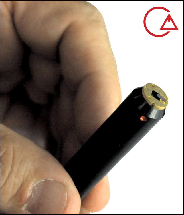
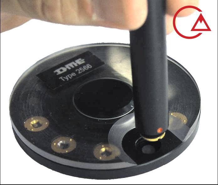
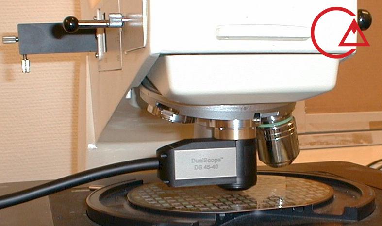
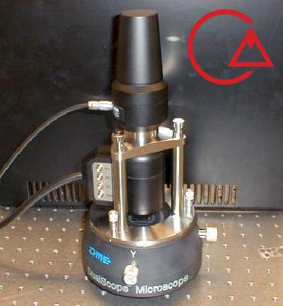
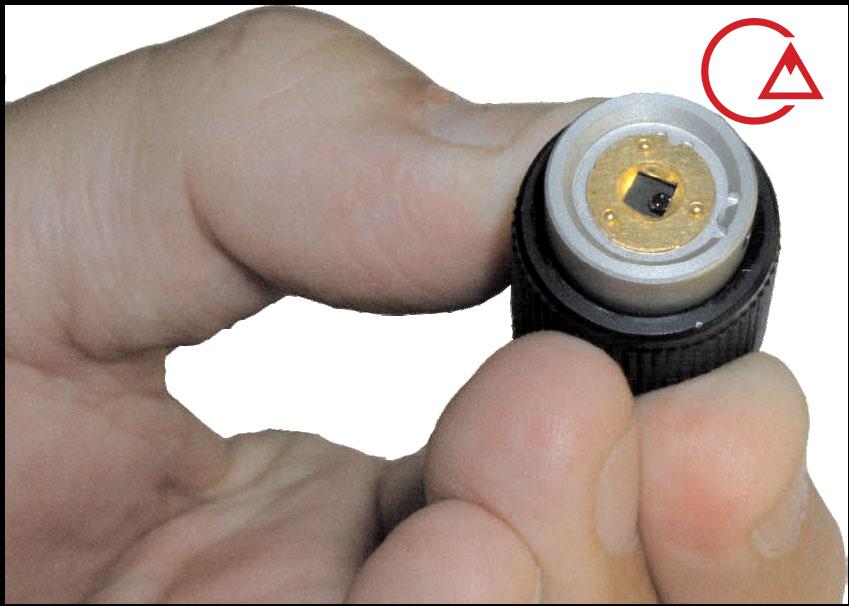
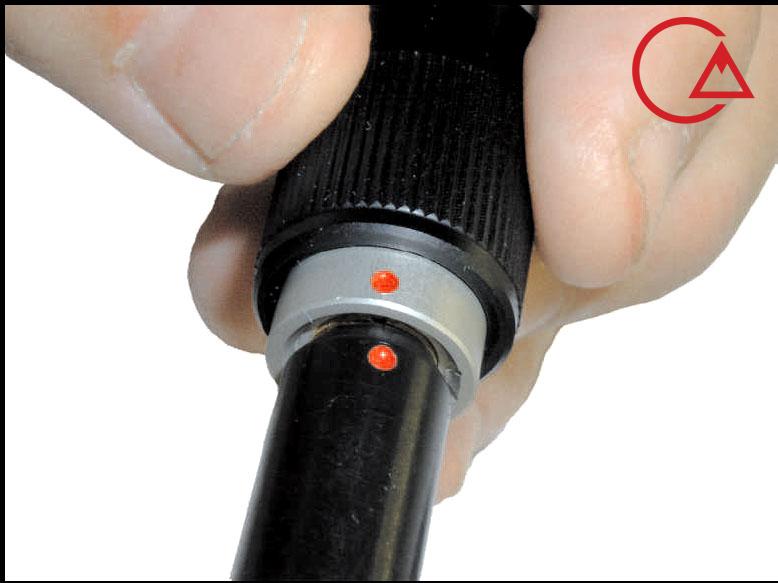
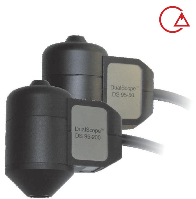
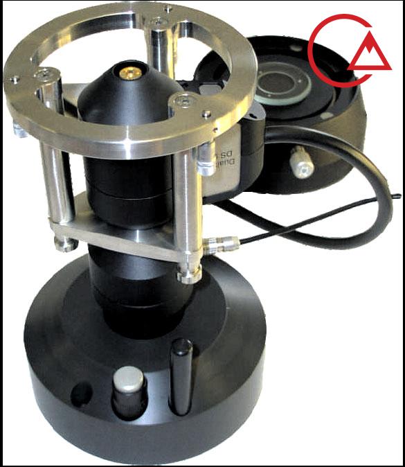
The combined scanning tunneling and atomic force device, which is also known as the scanning probe, is a combination of two STM and AFM devices. In this device, the imaging mode can be changed by replacing the cantilever connected to the device cap.
In this device, in comparison with other models, it is possible to change the imaging mode easily and only by changing the tip. Therefore, the general mechanism of this device is as follows.
A- STM system has modes
– Constant current imaging
– Fixed height imaging
– Spectroscopy IV
– IZ spectroscopy
– Tunnel flow lithography
– 8um transverse scanning range with 0.12nm drive resolution
– 3um vertical scrolling range with 0.05nm drive resolution
B- AFM system with modes
– Fixed height contact imaging
– Fixed force contact imaging
– Output of topography, vertical and lateral force for contact modes
– Semi-contact imaging
– Non-contact imaging
– Simultaneous output of topography, amplitude, phase, for both semi-contact and non-contact modes
– Atomic force spectroscopy
– AFM lithography
– 16um transverse scanning range with 0.24nm drive resolution
– 4um vertical scrolling range with 0.061nm drive resolution
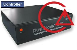
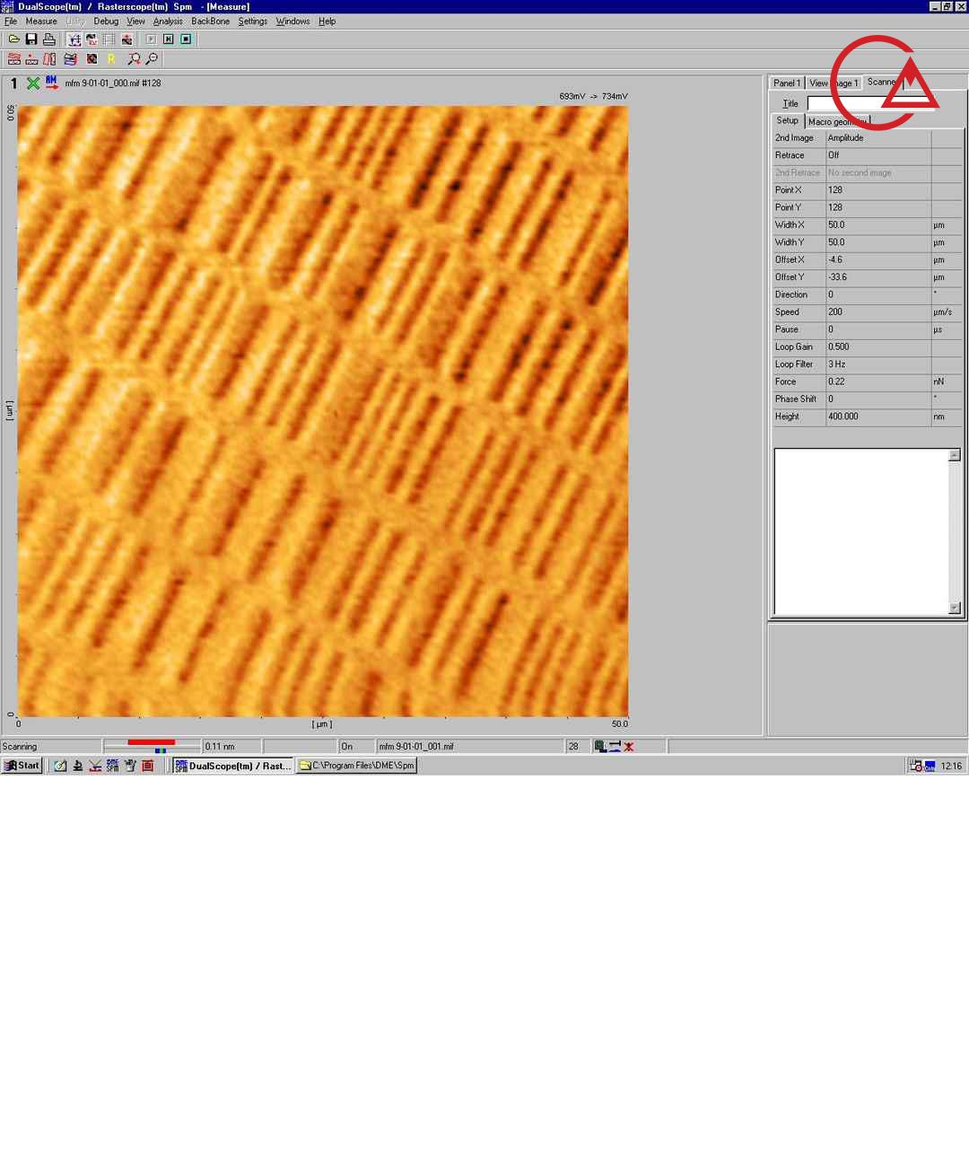
The various components of the device include a computer device and a single electronic case and two separate heads for STM and AFM that the user can connect and use one of the heads to the system according to his needs.
Description :
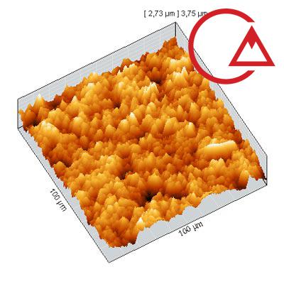
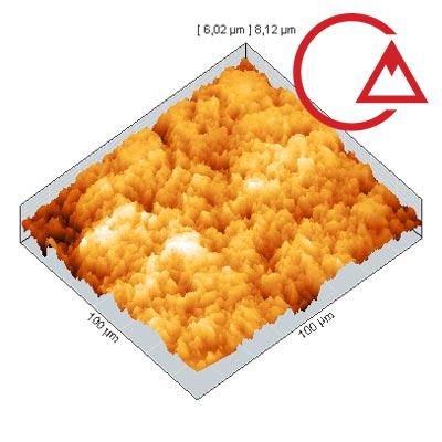
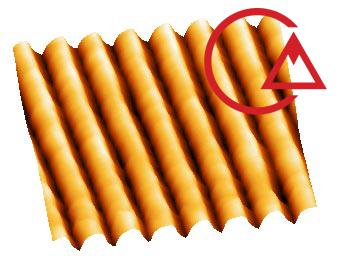
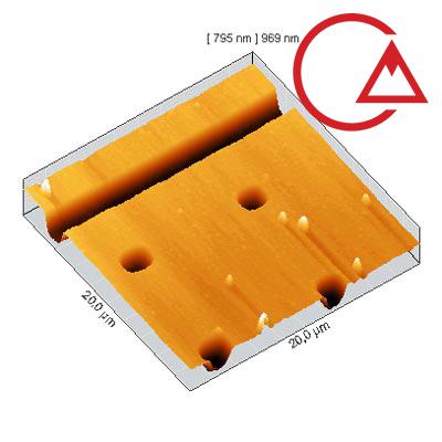
Scanning Probe Microscope: Scanning Probe Microscope (SPM) or Scanning Probe Microscope is a general term for a set of techniques that scan the surface of the material with resolution on the nanometer scale or even less than angstroms and topographic images or maps of It provides a physical or chemical property of the surface of the material. In this technique, like other scanning microscopy methods such as scanning electron microscope ( SEM ), the surface of the sample is scanned by a needle or probe, and by measuring and processing the signal obtained from different points of the scanned surface on the sample, the image of that surface is prepared. . The resolution and magnification of the scanning probe microscope is better than conventional electron microscopes, and it also provides the ability to produce 3D images of atoms. In addition to creating an image, this technique also allows the movement of atoms. Unlike most common electron microscopes that require vacuum and sample preparation, scanning probe microscopes work in air or under the liquid surface in addition to vacuum and with minimal sample preparation (and in some cases no preparation). do This fact, along with the possibility of measuring and using different signals for imaging, provides the possibility of examining a wide range of hard, soft, conductive, semiconductor, insulating, magnetic, etc. materials. As a result of this technique, along with other research devices, it has been widely used in various fields of metallurgy, ceramics, physics, chemistry, electronics, polymers, pharmaceuticals and biology.


Scanning Probe Microscopy SPM Scanning Probe Microscopy SPM